|
Читайте также: |
The Design of Three-stage BJT Operation Amplifier
Variant 2
Prepared by:
Second-year student
Group IACS – 208
Yatsura Anastasiya
Kyiv – 2013
Content:
Theory about the design of three-stage BJT operation amplifier
1. Design of an operational amplifier using a CA 3096 n-p-n/p-n-p transistor array.....................................................................................................................3
1.1. Five-transistor operational amplifier: dc analysis.................................3
1.2. Five-transistor operational amplifier: ac analysis.................................5
1.3. Class B power amplifier............................................................................7
Problems and individuals data.....................................................................................10
Calculations..................................................................................................................11
Conclusions…………………………………………………………………………4
List of references...........................................................................................................5
The purpose of this project is to design a three-stage BJT operational amplifier.
I. THEORY 1. Design of an operational amplifier using a CA 3096 n-p-n/p-n-p transistor array
We will design an operational amplifier using a CA 3096 IC, which is an n-p-n/p-n-p transistor array consisting of three independent but matched, n-p-n transistors and two independent, but matched, p-n-p transistors. This is an IC in that all emitters, bases and collectors are separately accessible as shown in Fig.1.

Fig. 1 CA 3096 n-p-n/p-n-p transistor array
Five-transistor operational amplifier: dc analysis
All three sections of a typical operational amplifier can be implemented with the five transistors in a single CA 3096, as shown in Fig. 2. A single-ended output of an emitter-coupled pair, Q1 and Q2, is used to drive Q4, a p-n-p common-emitter amplifier. The n- p-n/p-n-p pair, Q3 and Q5, represents a class В amplifier driven from the collector of Q4. A resistor is used to provide the current IEE. Since the typical hFE values for the n-p-n and p-n-p transistors are 188 and 45 respectively, all base currents will be neglected. It is also assumed that for vid = 0, v0= 0. The quiescent currents and voltages are obtained assuming both bases are grounded.

Fig. 2 CA 3096 connected as operational amplifier
Assuming that the base of Q1 is grounded, the current IEE is found by writing the KVL equation around the following loop: base of Q1, R3, VEE, and ground. So,

Because vO= 0 when viD = 0, then VC4 must be zero (this is input voltage to the output stage), which means that

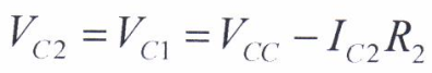
Biasing for Q4 is established by arranging VC2 to be sufficiently below VCC that VEB4 = 0.6V. To accomplish this,

and finally

Because Q1 and Q2 are matched and IB4 << IC2,
Дата добавления: 2015-10-31; просмотров: 178 | Нарушение авторских прав
| <== предыдущая страница | | | следующая страница ==> |
| Ожидаемые итоги и временные рамки | | | Class B power amplifier |