|
Читайте также: |
Consider in detail the class B amplifier operation (Q3 and Q 5). In Fig. 5, the circuit diagram of the output section is shown. The transfer characteristic of the output section is shown in Fig. 6.
The transistors are operated from the power supplies of equal voltage magnitude, VCC. The output signal, v0 (t), will be obtained as a function of the input signal, vI (t) = Vm sinωt. For vI = 0, both Q3 and Q5 are OFF; i C3 = iC5 = 0, and as a result, v0 = 0. As vI increases positively, Q5 remains OFF, and when vin > VBE(ON), Q3 turns ON. During this interval, Q3 operates as an emitter follower, where
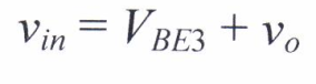

Fig. 5 Output class B amplifier

Fig. 6 Class B amplifier transfer characteristic
The output voltage maximum is
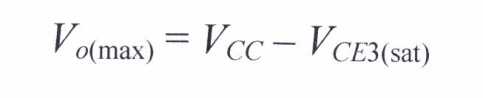
The input voltage necessary to drive v 0 to VCC - VCE3( sat) is given by

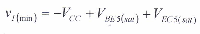
In most circuits, because v1 cannot exceed VCC, Q3 never saturates since VBE(ON) > VCE(sat). As v1 becomes negative, Q3 remains OFF, and when v1, drops below VBE5(ON) = 0.7V, Q5 turns ON. Transistor Q5 now behaves as a p-n-p emitter follower:

And it occurs for an input voltage of
As seen from Fig. 6, there is the 1.4-V dead band in the center of the characteristic. Such transfer characteristic leads to a distorted output waveform. This is so called crossover distortion shown in Fig. 7.
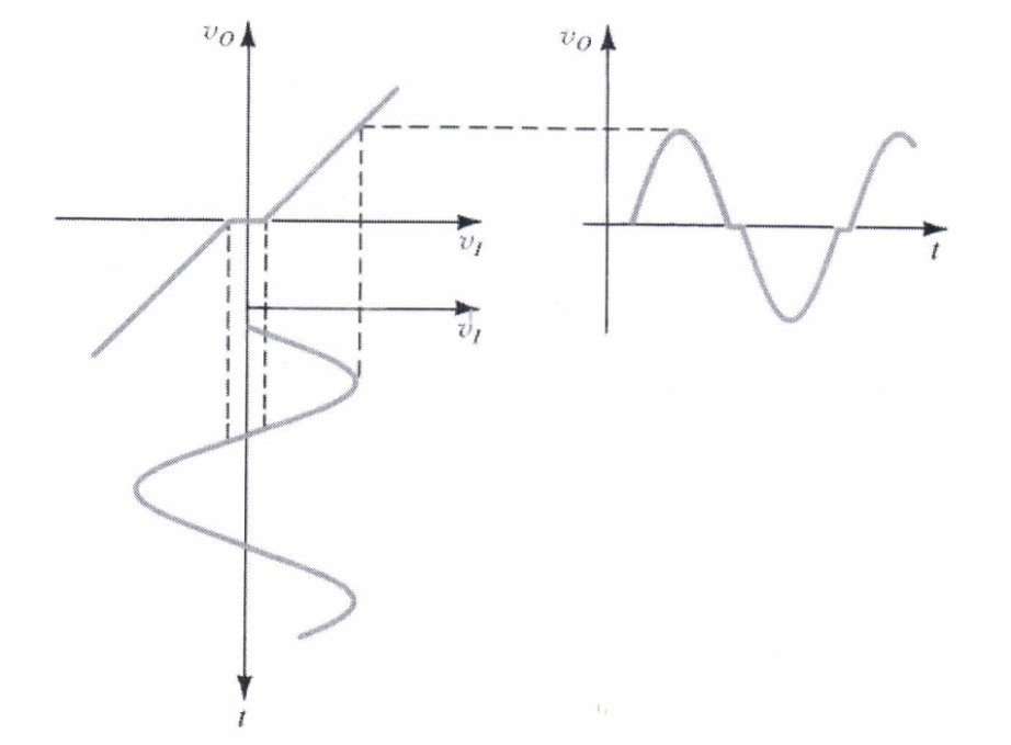
Fig. 6 Illustrating how the dead band in the class В transfer characteristic results in crossover distortion
II. PROBLEMS AND INDIVIDUALS DATA
Using a CA 3096 transistor array, design an operational amplifier to obtain a voltage gain AV =  if VEE = VCC, VBE1 = VBE2 = VBE3 = 0.7V, VBE4 =VBE5 = - 0.7V, VT = 26mV, β 1= β2= β3= 188, β4 = β 5= 45, and RL= l0kΩ. The resistor values should be compatible with the monolithic IC fabrication technology, i.e. any resistor value must not exceed 50kΩ.
Required voltage gain  = 275;
Power supply voltage VEE=VCC=12V;
The voltage gain of the designed operational amplifier must satisfy the following inequality:

a. Determine R1,R2, R3, R4, and R 5;
b. Calculate AV1, AV2, and AV;
c. Compute Rid, Ric, Ro3, and Ro5.
Дата добавления: 2015-10-31; просмотров: 114 | Нарушение авторских прав
| <== предыдущая страница | | | следующая страница ==> |
| Five-transistor operational amplifier: dc analysis | | | rdNR in RA- is MOTOR NR. ( in ventral horn of sp. cord). |