Читайте также:
|
The term photoelectric effect is applied to electrical phenomena occurring when a substance is illuminated with light. There are three types of photoelectric phenomena: 1) external photoeffect, when the absorption of light leads to the liberation of electrons beyond the irradiated body; 2) internal photoeffect, when the number of free electrons increases inside the matter, but they do not escape outside; 3) photovoltaic effect, when under action of radiation an electromotive force originates at the border of two semiconductors.
Striking out of electrons under the action of electromagnetic waves define important confirmation of the indispensability of the corpuscular viewpoint. Since the escape energy of an electron from a metal is not least than 2.2 eV, the photoelectric effect becomes possible when
 , (10.4)
i.e., for frequencies of the order of
 (λ=6.000 Å). (10.5)
Einstein proposed that the photoelectric effect be viewed as an effect of collision between a photon and an electron. If A represents the work function of electron, i.e. the work required to overcome the binding free between the electron and the substance, the low of conservation of energy has the form
 , (10.6)
where  is the kinetic energy of the photoelectron, the electron dislodged from the substance.
The variation of the electrical resistance of a semiconductor sample due to illumination is termed photoresistive effect, or internal photoeffect. The variation of the resistance or the conductance is caused by the variation of charge carrier concentration. The photoresistive effect may be described with the aid of photoconductivity σ pc
 , (10.7)
where d n, d p are excess electron and hole concentration produced by illumination. The conductivity σ 0= σ d due to equilibrium carriers is termed dark-current conductivity:
 . (10.8)
The total conductivity may be represented in the form of a sum of dark and light conductivities:
 . (10.9)
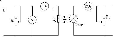
The electric circuit shown in fig. 10.1 may be used to measure the dependence of current of photoconductivity versus a different of voltage or a value of illumination on the photoresistor R 0.

Figure 10.1
Дата добавления: 2015-10-29; просмотров: 117 | Нарушение авторских прав
| <== предыдущая страница | | | следующая страница ==> |
| Порядок виконання роботи | | | ЛАБОРАТОРНА РОБОТА № 84.2 |