|
Читайте также: |
NATIONAL AVIATION UNIVERSITY
Radio Electronics Engineering Department
Course: Computer-Aided Design of Microwave Analog Cells
Experiment №2
The design and simulation of MOS single-stage amplifier in 0.12μm CMOS technology
Prepared by:
Anna Tarkovska IACS - 512
Kiev-Ukraine
Objective:
The purpose of this experiment is the design and simulation of MOS single-stage amplifier in 0.12μm CMOS technology.
Available software:
Lite version of Microwind
PROCEDURE
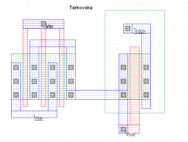
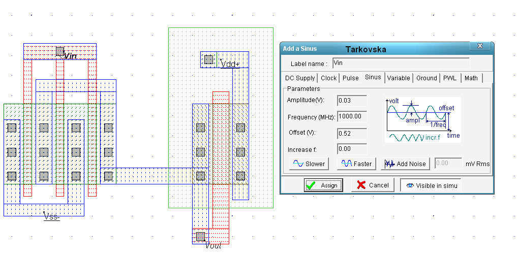
1. Design a single stage amplifier layout with a pMOS as a load resistor operating at frequency 2.5 GHz. Assume the amplitude of the input sinusoidal voltage of 50 mV. Select appropriate offset for the input signal providing maximum amplification. Let WN=3.6 μm, LN=0.12 μm, WP=1.2μm and LP=0.24 μm.

Create nMOS transistor. Assume WN=3.6 μm, LN=0.12 μm.

Add pMOS transistor (WP=1.2μm and LP=0.24 μm) and connects with pMOS transistor.

Details Vin+Vin, Vout, Vss, Vdd parameters.

Assume amplitude 0,03 (V) and offset voltage 0,52 (V).

Diagrams voltages and currents.

Diagram voltages vs. voltage.

Fast Fourier Transform of Vout.
2. Design a single stage amplifier layout for the same conditions as in step 1except that nMOS transistor has three fingers.

Create three fingers nMOS transistor. Assume WN=3.6 μm, LN=0.12 μm.

Add pMOS transistor (WP=1.2μm and LP=0.24 μm) and connects with pMOS transistor
Details Vin, Vout, Vss, Vdd parameters.
Assume amplitude 0,03 (V) and offset voltage 0,52 (V).

Diagram voltages vs. voltage.

Diagrams voltages and currents.

Fast Fourier Transform of Vout.
Conclusions
The single stage amplifier may consist of a MOS device (we choose here an n-channel MOS) and a load. The load can be a resistance or an inductance. In the circuit, we use a resistance made with a p-channel MOS device with gate and drain connected. The pMOS which replaces the passive load is called an active resistance.
The goal of the amplifier is to multiply by a significant factor the amplitude of a sinusoidal voltage input Vin, and deliver the amplified sinusoidal output Vout to a load.
What we need is to find the characteristics Vout/Vin in order to tune the offset voltage Vin. The range of voltage input that exhibits a correct gain appears clearly. Change the parameter Offset of the input sinusoidal wave to place the input voltage in the correct polarization. We change the sinusoidal input offset and start again the simulation.
Дата добавления: 2015-10-29; просмотров: 89 | Нарушение авторских прав
| <== предыдущая страница | | | следующая страница ==> |
| La paire de chaussures | | | Лабораторная работа №3 |