Читайте также:
|
Contacts phenomena on p-n junction
THE AIM: to study the electrical conductivity of p-n junction.
THE TASK: plot the volt-ampere characteristic of p-n junction.
INSTRUMENTATION AND APPLIANCES: voltmeter, milliampermeter, source of current, diode.
Introduction
The classification of materials according to their conductivity materials are characterized by different conductivities, table 14.1:
Table 14.1
| Material | σ, s˙m-1 |
| Aluminium | 3.12˙107 |
| Gold | 4.13˙107 |
| Copper, drawn | 5.62˙107 |
| Copper, annealed | 6.30˙107 |
| Silver | 6.03˙107 |
| Nichrome | 9.00˙105 |
| Diamond | 10.00˙10-10 |
| Ebonite | 5.00˙10-14 |
| Pyrex | 1.00˙10-12 |
| Micx | 1.10˙10-11 |
| Paraffinized wax | 3.30˙10-17 |
| Quartz | 5.10˙10-13 |
Materials with conductivities σ =(107÷106) S˙m-1 are usually termed conductors, or metals.
Isolators or dielectrics are those with conductivities σ =(10-8÷10-16) S˙m-1.
Materials with intermediate conductivities σ =(10-8÷106) S˙m-1, were termed semiconductors.
The temperature dependence of conductivity of metals is the resistance increases with temperature:
 . (14.1)
here R 0 is the resistance at t = 0° C; α is the thermal resistance coefficient equal about 1/273.
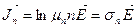
In case of semiconductors the resistance rapidly decreases with the increase of temperature. The empirical formula connecting the resistance and absolute temperature T valid within a limited temperature range is given below:
 , (14.2)
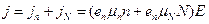
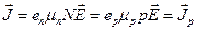
where B is constant. This formula may be rewritten for conductivity
 , (14.3)
where k is Boltzmann's constant. The quantity E a characteristic of the given semiconductor is called its activation energy.
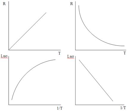
Figure 14.1
The semiconductors are materials the conductivity of which at room temperature ranger between 10-8 and 106 S˙m-1 and depends strongly on the nature and amount of impurities, on the structure of the material and on the ambient: temperature, illumination, electric and magnetic fields, etc.
There are two kinds of semiconductive materials: ionic and electronic. In ionic semiconductors the current is carried by the ions of the substance.
The current in electronic semiconductors is carried by electrons only. A crystal lattice is a result of atomic interaction. The nature of this interaction is determined by the atoms costituting the crystal. Main part in this interaction is played by the so-called exchange effect in the course of which two atoms exchange electrons and there by establish forces of attraction between them.
Let us discuss the model of conduction in semiconductors using silicon as an example.
The silicon atom has 14 electrons, which are divided among the electron shells in the following way: (1s2)(2s2)(2p6)(3s2) 3p2. The incomplete outer shell contains four electrons. The lattice type of the silicon crystal is the diamond type. The diamond-type lattice is cubic. Every atom is bound to four nearest silicon atoms by covalent bonds, and all of its four valence electrons take part in these bonds. In the ideal lattice all electrons are bound, there are no free carriers, and, correspondingly, the application of an electric field does not result in an electric current. To produce current some electrons must be freed from their bond. To tear an electron away from its bond energy must be expanded. This energy may be supplied to the crystal in the form of the energy of photons, or of particles, or in the form of the energy of thermal lattice vibrations. At room temperature the energy needed to free one electron in silicon is 1.08 eV. Note that the freeing of one electron produces one incomplete bond.

Figure 14.2
The process of bonding a free electron is termed recombination. It is the opposite of the process of freeing a bonded electron. The number of free electrons and vacant (incomplete) bonds are equal.
If electric field  is applied to the crystal, free electrons taking part in random thermal motion will be acted upon by the force
  and will begin to drift against the field. If we denote electron concentration by n, their mobility by μ n, we will be able to write for the electron current density.
 . (14.4)
The incomplete bond can, in fact, move from atom to atom as a result of electron motion. When external electric field is applied the bound electrons will be acted upon by the force  and will be moving against the field and occupy vacant bonds. The availability of vacant bonds enables valence electrons to move against the field. This means that their mobility depends on the number of vacant bonds usually called holes. In this way the mass of the valence electrons, too, contributes to semiconductor conductivity.
If the concentration of bound electrons is N and their mobility μ n, their current density is
 . (14.5)
Thus, in semiconductors there are two kinds of charge carriers: free electrons and bound electrons.
Therefore
 . (14.6)
The motion of the hole in the direction of the field is equivalent to the motion of a positive charge e +. Denoting the hole concentration by p and their mobility by μ p, we can write the current density of the mass of bound electrons in the form
 . (14.7)
Holes with the charge e p = e + are regarded as quasiparticles the motion of which is quite equivalent to the motion of valence electrons.
A semiconductor with equal concentrations of electrons and holes (n = p) is termed intrinsic. The current density in it is
 . (14.8)
Difference of concentrations of electrons and holes is produced by introducing impurities, also called doping. This leads to extrinsic (impurity) conductivity. To understand the essence of extrinsic conductivity let us consider silicon doped with elements of the fifth and the third groups. Suppose an arsenic atom replace silicon atom in the crystal lattice. The outer shell of the arsenic atom has five electrons. Four of them will take part in forming covalent bonds with nearest silicon atoms. The fifth electron is unable to take part in bonding since all the bonds are filled. At the same time it is acted upon by the neighboring silicon atoms hence the decrease if its bonding energy to the arsenic atom.
For this reason impurities are easily ionized, and a large number of free electrons appear in the crystal – much larger than in pure silicon.
Impurities, which supply electrons, are termed donors. The donor impurity acts only as a source of free electrons.
The concentration of electrons in a donor-doped semiconductor will be much greater than the concentration of holes. Current in such a crystal is carried mainly by electrons by reason of which they are termed majority carriers, while the holes are termed minority carriers. Such a semiconductor bears the name of electron, or n-type semiconductor. The conductivity of an electron-type semiconductor may by written in the form
 , (14.9)
since p << n and σ p << σ n.
Consider now another case. Suppose an atom of indium, or any other group III element, is introduced into silicon. The indium atom has three valence electrons by reason of which one of its bonds with silicon atoms will remain incomplete. To fill this bond it is necessary to transfer to the indium atom one electron belonging to some silicon atom.
An impurity atom, which accepts an electron, is termed acceptor. In a semiconductor, doped with acceptors the hole concentration greatly surpasses the free electron concentration, and because of this its conductivity is mainly of the hole type:
 , (14.10)
since n << p and σ n << σ p. In this case holes are majority carriers and the electrons-minority carriers. An acceptor-doped semiconductor is termed hole, or p-type semiconductor.
14.2 Inhomogeneous semiconductor, p-n junction
We may consider the contact between an electron and hole-type sample of the same semiconductor.
Suppose we have a semiconductor sample with donor N (r) and acceptor N (r) impurities arbitrarily distributed in it. This results in electron and hole concentrations being dependent on the coordinate.
The diffusion current  results in charge separation leading to the creation of a space charge and of the accompanying electric field, which bends the energy bands. In thermodynamical equilibrium the Fermi level is independent of the coordinate:
 . (14.11)
The diffusion current is compensated by the drift current  therefore
 . (14.12)
Some electrons from n -region will go over to the p -region, and some of the holes from the p -region will go over to the n -region, charging the n -region positively, and the p -region negatively.
An electric field will be established in the p-n junction area directed from the n-region to the p -region.
The resistance of a semiconductor with built-in-fields and space charges measured for opposite current directions will be different. An external voltage applied to a p-n junction drops almost entirely on the space charge region. Let the external field be directed against the contact field E c. The external electric field lowers the potential barrier U c with the result that the electron flow from the n-region increases almost exponentially with the applied voltage. When the direction of the applied voltage is reversed, the electric field raises the potential barrier with result that majority carriers are drawn away from the junction region, and the width of the space charge layer is increased. The current through the junction consists only of minority carriers whose concentration is small, and for this reason the current termed reverse current is also small.
Even though the boundary between two bodies in close contact (welded or fused) is very narrow, nevertheless it is of finite width; hence the designation barrier layer. Investigations indicate that a barrier layer between two semiconductors is formed when one of the semiconductors is a p -type conductor and the other an n -type. Such barrier layer is called p-n junctions, fig. 14.3.
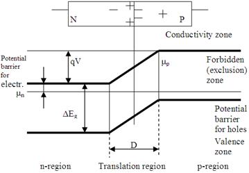
Figure 14.3
Figure 14.4 illustrate the rectification provided by barrier layers. The figure shows a typical current-voltage curve. The left branch of the curve is the characteristic for the reverse current. The forward current increases rapidly with increasing voltage, but the reverse current remains almost constant and has vary low value.
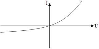
Figure 14.4
Дата добавления: 2015-10-29; просмотров: 193 | Нарушение авторских прав
| <== предыдущая страница | | | следующая страница ==> |
| ЛАБОРАТОРНА РОБОТА № 85 | | | Experimental part |