Читайте также:
|

|
| The semiconductor crystal is composed of a large number of periodically positioned atoms of which the former energy levels split into a large number of closely neighboring levels. These energy states form the so-called " bands " that are separated by band gaps. |

|
| In the ground state, the bands are filled up with the existing electrons, according to the Pauli principle, beginning with the lowest energy. The highest completely populated band is called the valence band, the next higher one the conduction band. |

|
| Joining a p - and an n -semiconductor creates a very thin p – n junction with locally shifted energy bands. To create a population inversion, necessary for optical gain and laser oscillation, an external electric field is applied to the diode (+ to p -type, – to n -type). |
Parabolic bands
E c = E c0+ ħ 2 k 2/2 m c energy of electrons
E v = E v0– ħ 2 k 2/2 m v energy of holes
E g = E c0– E v0 energy gap
Density of states
rc(E c) = (1/2p2) (2 m c/ ħ 2)3/2 (E c– E co)1/2 (cm-3 eV-1)
Fermion statistics
Fermi–Dirac functions
f e(E c) = (1+exp(E c– F e)/ kT)-1 
f h(E v) = (1+exp(F h– E v)/ kT)-1 = 1– f e(E v), 
kT thermal energy
F e quasi-Fermi level for electrons
F h quasi-Fermi level for holes
Δ F = F e– F h
Carrier concentrations
n = N c F 1/2(ζc/ kT)
ζc = F e– E c0 chemical potential for electrons
N c ~ (m c kT)3/2 effective density of states (cm-3)
F 1/2(ζc/ kT) Fermi integral of index 1/2
Analogically we have for holes
p = N v F 1/2(ζv/ kT)
ζv = E vo– F h chemical potential for holes
N v ~ (m v kT)3/2 effective density of states (cm-3)
n, p ~ T 3/2
n p at F e and F h ¯ or Δ F = F e– F h (excitation level)
At thermodynamical equilibrium we have Δ F º 0.
Inversing condition (optical gain and lasing): Δ F ³ E g
Electron impulse space in crystalline semiconductors

Brillouin zone of the face centered cubic lattice, the Bravais lattice of the diamond and zinc blende structures.
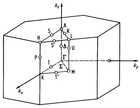
Brillouin zone of the hexagonal lattice.
Elementary semiconductors
Si received in pure matter by Bercelius (Sweden) (1825)
Ge obtained by Winkler (Germany) (1886),
predicted by Mendeleyev (Russia) (1871)
Дата добавления: 2015-10-29; просмотров: 172 | Нарушение авторских прав
| <== предыдущая страница | | | следующая страница ==> |
| Рекомендации по заполнению таблицы | | | Expérience 2. Le rôle de la sérum-albumine au cours du transport des acides gras supérieurs dans le sang. |