Principle of f.e.t.
Consider the f.e.t. with batteries connected as shown in Fig. 39.25. The potential of the drain D is +ve relative to the source S, so the electrons in the n-bar flow from S to D. This current is called the drain current ID.
The battery between the gate G and S makes the potential of G — ve relative to S. Now the n-bar near the p-junction has a +ve potential relative to S. Thus the p-n junction near the gate is reverse-biased. Consequently, as shown diagram-matically in Fig. 39.25, a depletion region is obtained at the p-n junction (p. 826). The width of the depletion region depends on the magnitude of the p.d. V GS when the p.d. V DS is constant. If V GS, is made more -ve the wider is the depletion region at the p-n junction. This is shown diagrammatically in Fig. 39.25.
The depletion region, which has no free electrons, narrows the conducting n-channel in the bar. When V GS is made more -ve, the current is reduced As it provides a sensitive control over the drain current, small changes in gate voltage can produce large amplification of the current. Thus signals, or a.c. voltages. can be amplified by the f.e.t. transistor.
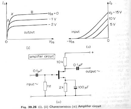
| When the gate voltage VGS is made more negative, the reverse-bias is increased. The current ID is now decreased. Figure 39.26 (ii) shows the effect on the input characteristics.
An a.f. amplifier circuit which uses the f.e.t. transistor is shown in Fig. 39.26 (iii). The load resistance is 10 kOhm, the temperature stabilisation is provided by the 2 kOhm resistance and the necessary bias for an undistorted output is provided by the 1 MOhm resistor. The 0.1 uF capacitors prevents direct current or voltage reaching the input and output circuits.
| |

| | | | |
| | | F.E.T. Characteristics. F.E.T. Amplifier
Some typical output characteristics (ID - VDS, VGS constant) and input characteristics (id - VGS, VDS constant) are shown in Fig. 39.26 (i), (ii).
When VGS is kept constant, the drain current ID first increases linearly as the voltage VDS is increased from zero, since the bar then acts as an ohmic conductor. This corresponds to the line A in Fig. 39.26 (i). When VDS increases further, the p-n junction at the gate becomes more reverse-biased, since the positive potential of the n-bar at the gate increases relative to S and hence relative to G. The depletion region then widens, as stated above, and so the current ID begins to increase at a slower rate. The slow rise of ID with VDS begins at X in Fig. 39.26 (i) and continues along the straight line B.
| |
| |
| | |  |
Дата добавления: 2015-10-31; просмотров: 101 | Нарушение авторских прав
Читайте в этой же книге: ДЛЯ 1-ГО КУРСА МО | Semiconductors. Movement of Charge Carriers | P- and N-type Semiconductors | Full Wave Rectification. Filter Circuit | Common-Emitter (C-E) Characteristics |
mybiblioteka.su - 2015-2024 год. (0.007 сек.)